Sunday, June 12, 2016

Momentum Space (Kspace) Final Project - Pending

In this project I will examine Fermi boundaries in Momentum Space or K-Space diagrams as they pertain to the lattice structure of various metal crystals.

Introduction 

A unique definition of a metal is one which has a Fermi Energy (\(E_f\)) in the conduction band. This is one property which gives metals such great conductivity, having an \(E_f\) in the conduction band means that electrons in the valence band can easily move to the conduction band. Unlike in a semiconductor or an insulator in which the \(E_f\) level lies between the band gaps this allows us to be able to model shift in \(E_f\) as a function of filled or occupied electron states.

Free electrons in the conduction band can be modeled by what are called Bloch states, the sum of which can be modeled by \(\psi_k(x)=\sum e^{inak}\phi (x-na)\). Of prime importance is what is called the "wave vector" \(k\) which can be manipulated to form Bloch states of varying symmetries. The wave vector \(k\)  is associated with the free electrons momentum state, we will examine what is called the "first Brillouin zone" defined as the range \(k=(\frac{-\pi }{a},\frac{\pi}{a})\).

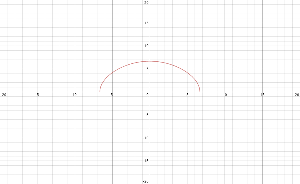
This unique transformation into momentum or Kspace allows us to view what are called "Fermi boundaries" or 2D Fermi Levels as visualized in Kspace. Each Fermi boundary is a line in the first Brillouin zone in Kspace and it is a line of constant energy which separates the filled (area bound inside the contour) to the unfilled states. If we look at the ratio of area within the Fermi boundary as a fraction of the total area in the first Brillouin zone we have calculated the fraction of filled states for a given \(E_f\) with our given lattice structure.

(For brevity of the post the Python code used to generate the animations and diagrams will be linked below, but all that is needed is here.)

Part 1: Simple Cubic Structure


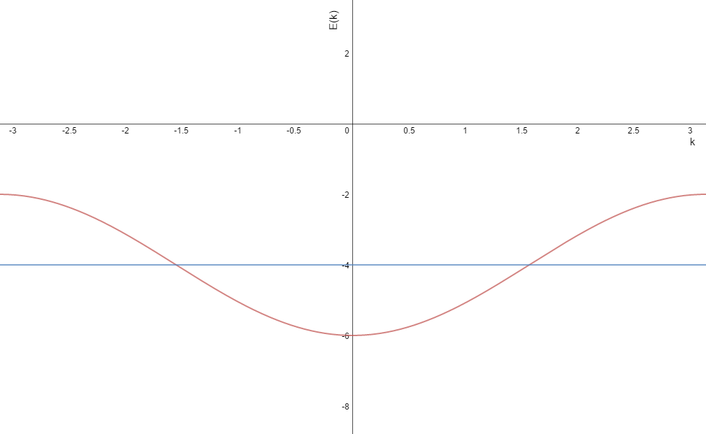
The first structure I will examine is that of a simple cubic lattice modeled by: \(E(k)=E_0-bcos(ak_x)-bcos(ak_y)\). From this equation we can deduce some important properties of this structure. Firstly it is symmetric in the x and y direction because we have both  -bcos(ak_x) and -bcos(ak_y)\) contributing equally to the term inside the Cosine function, that is both terms are equal for \(ak_x = ak_y\). Another thing to note is that the lattice constant \(a\) is not changed in either term meaning that the spacing in the x and y direction does not differ.

Lastly we have a range of \(E(k) = (E_0+2b,E_0-2b)\). This is expected for our case as it is symmetric and cubic and we expect the range to be the same above \(E_0\) as below.
This is important as we shall soon see that for varying structures of metal crystals the range of the band width changes.


The Kspaces in the animation are well organized into half circles which gradually become more and more triangular. Of particular importance is \(E(k) = E_0 + 0\) this is a special Fermi boundary which I will refer to here as the "prime" energy of \(E_p\). In the plot below the animation  \(E_p\) occurs at the center of the graph which is also the point at which the graph switches concavity, it is a point of inflection.

These points of inflection are where the filling of states changes from increasingly more sates per \(E(k)\) to decreasing change in states filled per \(E(k)\).

Visually these points of inflection are of great interested in Kspace diagrams as they are the ONLY Fermi boundaries created with straight lines. In the animation above this occurs where the perfectly straight triangle is drawn at \(E(k) = E_0 + 0\). We will examine more of these special  \(E_p\) energies for other crystal structures.

Part 2: Anisotropic Case


For a structure that is anisotropic (meaning it varies along the x and y axis) we look at: \(E(k)=E_0-bcos(a_xk_x)-\frac{b}{4}cos(a_yk_y)\). This equation models that of a crystal lattice structure similar to that of Part 1 except that here we let the lattice separation \(a\) be different along the x and y directions. Not only did we break the symmetry along the x and y directions we also allowed for a different "weight" in the y direction by the addition of multiplicative constant of \(\frac{b}{4}\). This means our crystal can have different separations in the x and y direction and it also creates a crystal in which we have the energy \(E(k)\) being heavily weighted in the x direction, that is the structure of this crystal would have more energy per change in \(k_x\) than per unit change in \(k_y\).

For lattice spacing (ax,ay):


For lattice spacing (ax,2ay):


For lattice spacing (2ax,ay):


In all three cases the graph of States Filled vs \(E(k)\) is exactly the same. The amount of electron states occupied in conduction band of the crystal does not depend on the spacing of the atoms in the crystal but is dependent only on the Energy. In all three cases we reach a Fermi boundary which contains half the total states inside it at exactly \(E(k) = E_0 + 0\), the same as in Part 1.

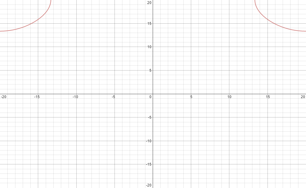
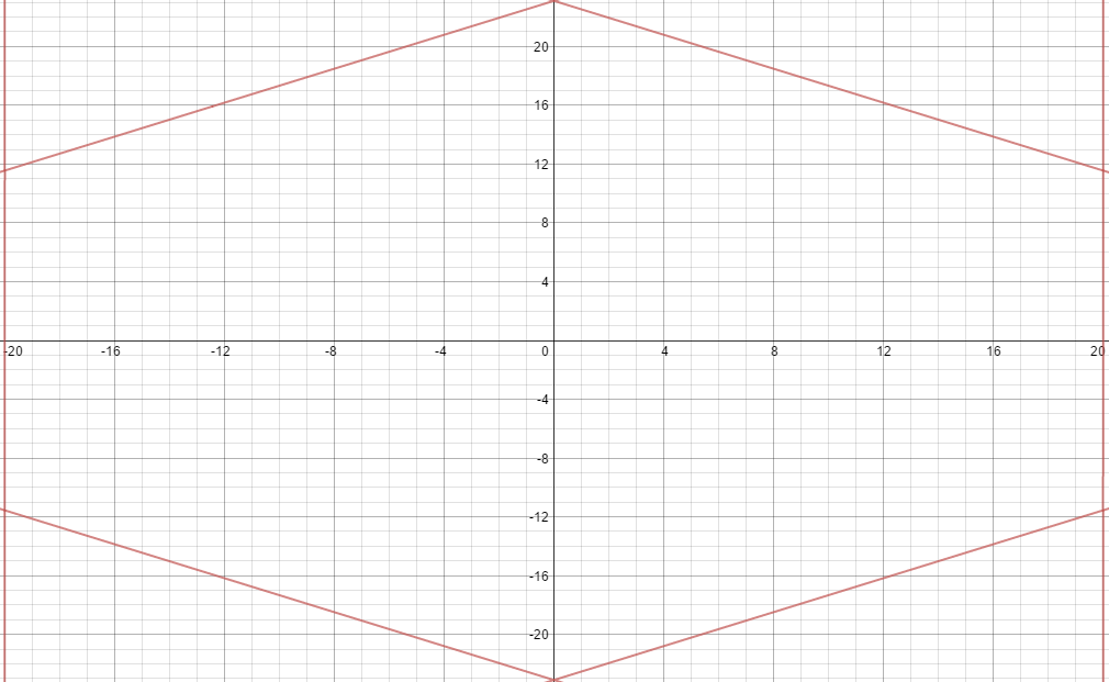
Here the similarities end and we can see that the anisotropic case has some very significant differences to that of Part 1. Firstly we can see that there are four curvatures and concurrently three points of inflection at \(E(k)= E_0 + (-1.5,0,1.5)\).


These are our \(E_p\) values yet with one notable exception at \(E(k) = E_0 + 0\)...in the anisotropic case symmetry has been broken and only some parts of the Fermi boundary formed at these values have straight lines.

There is also now a change in the range of \((k_x,k_y)\) as we no longer have \(E(k) = E_0 + 2b\) or \(E(k) = E_0 - 2b\) as in Part 1. In the anisotropic case \(E(k)\) still ranges in the \(k_x\) direction by \((+/-)b\) but now as we have discussed it only ranges by \((+/-)\frac{4}{b}\) in the \(k_y\) direction. We can then see as the animation and plots above show that the total energy \(E(k)\) ranges only between \(E(k)=E_0-\frac{5}{4}b\) and \(E(k)=E_0+\frac{5}{4}b\).

In essence this crystal structure has a narrower energy band as the energy difference between 0% states filled and 100% is reduced from the simple cubic structure and we need only a band width of \(\Delta E(k) = 2.5b\). This is true even in the case where our lattice structure has \(a_x = a_y\) as we see in the first case above.


Part 3: Complex Structure

Lastly the case which more closely models a real world metal crystal structure: \(E(k)=E_0-bcos(ak_x)-bcos(\frac{1}2{}ak_x+\frac{\sqrt{3}}{2}ak_y)-bcos(\frac{-1}2{}ak_x+\frac{\sqrt{3}}{2}ak_y)\)

This case has unique properties which seem to derive from those of Parts 1 & 2. The range of \(E(k)\) is skewed to the negative end because the equation \(E(k)=E_0-bcos(ak_x)-bcos(\frac{1}2{}ak_x+\frac{\sqrt{3}}{2}ak_y)-bcos(\frac{-1}2{}ak_x+\frac{\sqrt{3}}{2}ak_y)\) can attain a lowest value of \(E_0-3b\) yet oddly it can not have a value of \(E_0+3b\), in other words it has broken the symmetry of the energy band width in the previous cases above.

This crystal structure also attains a higher compaction of electron states as shown in the plot below the animation. In the plot we can move from \(E_0+1\) to \(E_0+3\) and increase the number of states filled by 40%, the same change in energy in Part 1 would yield only a change of about 22%.

This case and the one in Part 1 have only one inflection point, in our case at \(E(k) = E_0 + 2\) which forms perfectly straight lines angled similarly in a triangle shape but with flat sides forming more of a top half of a hexagon.

Part 3: \(E_p\) and crystal structure


Kspace diagrams have been shown above in deducing the fraction of total electron states occupied in varying crystal lattice structures in a metal, but one can also look at the structure or arrangement of the lattice structure by looking at what I have called the "prime" energy \(E_p\).

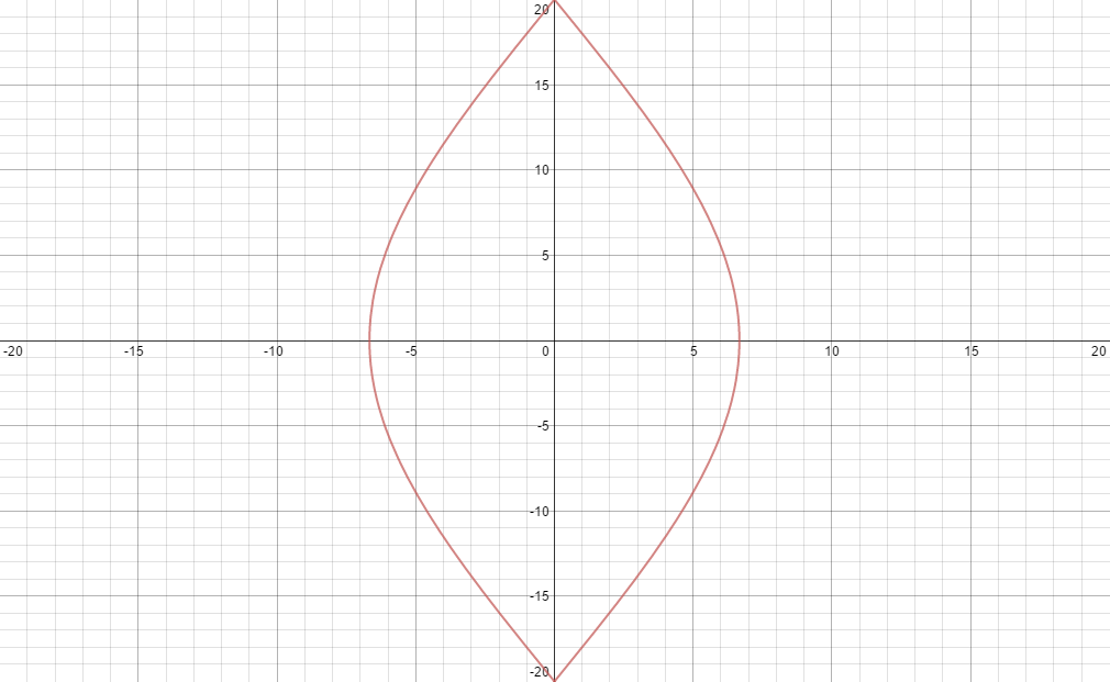
In case Part 1 our \(E_p = E_0 + 0\) yields a Fermi boundary which if we look at the entire first Brillouin zone looks like a diamond as shown below:

and in Part 3 we have our hexagonal \(E_p\)


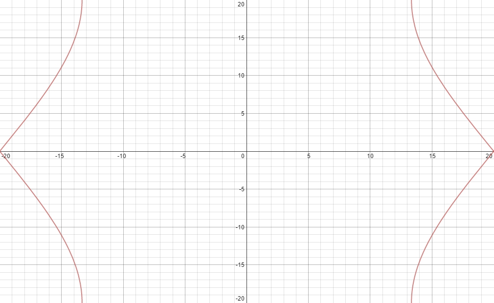
In Part 1 the structure shown is a square at  \(E_p\) and this is exactly what we expect for a simple cubic structure, that is one atom surrounded by 4 others on each side. Simple periodic and symmetric about x and y. We can expand our view of the first zone of our function to include nearby neighbor and we can see the simple cubic structure appears as below.
In Part 2 we have \(E_p\) is a hexagonal structure. This is consistent with a more compact structure as we have determined from the data in Part 2. Again viewing the structure at \(E_p\) yields a symmetric period hexagonal structure where each atom is surrounded on each of it's six sides by another.

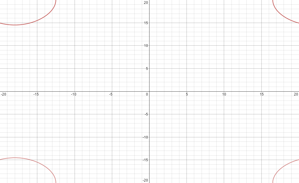
The anisotropic structure in Part 2 seems rather out of reach visually yet there are some important revelations about its Kspace diagram namely, as we have found, that it has not 1 but 3 points of inflection two of which are special cases where the Fermi boundary satisfies the condition of being an energy of \(E_p\) at  \(E(k)= E_0 + (-1.5,0,1.5)\). 

For Parts 1 & 3, we have only one\(E_p\) Fermi boundary and concurrently only 1 point of inflection on the plot of states filled vs E. This lead us to deduce the structure of the lattices formed. 

So what does it mean to have multiple \(E_p\)? And how can we understand its structure in this case.
We know that Parts 1 & 3 have only one \(E_p\) Fermi boundary (Diamond and Hexagon respectively) but for our anisotropic case we have the three below:
E_0 -1.5
E_0+1.5
All but the center graph contains areas where the Fermi Boundary has some linear sections but it is still very distinctly different from that of Parts 1 & 3. If we follow the methods in Parts 1 & 3 it is only logical to determine that for our anisotropic case we have a lattice which is not symmetric or pattern like, unlike in Parts 1 & 3 we can not deduce the structure from only one \(E_p\). 

We must then make the conclusion that this lattice structure has a broken symmetry, that is, unlike in Parts 1 & 3 which look the same along any direction, in the anisotropic case we have one symmetry along one x axis and another along the y axis. Below I have expanded out the first Brillouin zone to show the lattice structure in this anisotropic symmetry.

As we have concluded the atoms are arranged in the y direction in rows each almost touching the other but in the x direction this symmetry is broken and a new symmetry takes place, one in which every atom is neighboring two others but not touching or at least not as closely packed as in the y directions.

Conclusion

Kspace diagrams are useful in examining the properties and structure of metal crystals as we have seen in 3 different cases. The cases studied here are very simple and in some cases unrealistic but they nonetheless showcase the usefulness of Fermi boundaries in Kspace for metals.

From the compactness of the electron states and their associated energy band width to the actually symmetry of the crystal lattice, all can be understood from the simple view in the momentum space diagrams of the Fermi boundaries.


References:
http://www2.phy.ilstu.edu/~marx/ph355/Kittel_Solid%20State%20Physics/c09.pdf
http://ucscphysics156-2016.blogspot.com/2016/04/this-may-be-pretty-difficult-and-long.html
http://ucscphysics156-2016.blogspot.com/2016/05/homework-on-fermi-boundaries.html
http://www.wolframalpha.com/


Wednesday, May 25, 2016

156 final project

I think for the final project you should pick a topic you like, discuss your choice, the reasons etc., and do a project on that, sort of like what Valentine has done in the previous post. Do some analysis, write some paragraphs about what interested you and what you learned...   How does that sound?

-Due around Thursday of finals week by email in pdf form (or scanned).

Super cool post Valentin!!!!!

I think something is wrong for the second python code, where you have the applied voltage.

I don't think that the way you applied the voltage will not change the lower limit of the band, it just moves it in the k-space.

The bottom of your band is -12eV, so even for E(k) = 11.5 eV, you get that some states are filled in the case with no applied voltage.


I think that for the case of an applied voltage of 2eV over the x-direction, the bottom of the band is  just moved a bit to the right, so you should have the same amount of filled states, as long as your E(k) < E_f.


But an applied voltage should actually lower (or rise) the bottom of the band so you should use a different b-value for the kx-section

\( E(k) = E_0 - scale \cdot b \cdot cos(a k_x) -  b \cdot cos(a k_y) \)
 where scale is the effect of the applied voltage.

Monday, May 23, 2016

Homework due date!

Hey everybody,

Christian and I talked with Zack earlier, and it is decided that for the time begin we'll focus our attention on FETs.

So, instead of finishing up the Fermi Boundaries assignment which was due on Wednesday (May 25th), we should be working on the problem discussed in class today. The Fermi Boundaries problem set will be due during the week of the 30th.

Sunday, May 22, 2016

Symmetric and Asymmetric Fermi Surfaces in Kspace

Valentin Urena Baltazar

Hi all! Welcome to my first post for our Physics 156: Solid State class!

IMPORTANT NOTE: Read this Introduction on the Blog and THEN click the links to Parts 1 & 2 at the bottom! They have all the really cool Kspace diagrams I plotted using Python! I also ask some questions there that you all can try and comment on here. Thanks!

First let us begin with  a little introduction to the related subject on this post.

We have been studying energy bands and their related electron states. We tackled 1 Dimension for which the \(E_F(Fermi)\) level is depicted below as two points that bound the electron states below them. For this 1D case we have E(k) as a function of just kx.


Efermi as the blue line

Now we have moved onto 2D models, that is now the \(E_F\) boundary is a line or lines in our \((k_x,k_y)\)space. These “Fermi surfaces” also relate to the energy in that the area within the contours is directly proportional to the fraction of electron states occupied. Everywhere along the contour the energy is constant and the electrons occupy states below that energy which in our \(Kspace\) plot would be the area within the bounds of the contour lines. The total area is always a square of side length \(2\pi /a\) but depending on the \(E_F\) level the area formed within the contours will be some fraction of the total area.

Let us begin with the simplest example: when we have half the total states filled as shown below.


(note: kx is along the X axis and ky along the Y axis for all 2D graphs posted)

The graph above shows the equation \(E(k)=E_0-bcos(ak_x)-bcos(ak_y)\) for the case where \(0=-bcos(ak_x)-bcos(ak_y)\) that is \(E(k)=E_0\). Which we know is the halfway point of our band which ranges from \((E_0-2b,E_0+2b)\)

We will use \(a=.157nm\), \(b=2eV\) and let \(E_0\) just be some constant.

Now the area shown above can be found 2 ways.
  1. Geometry! It looks like 4 right triangles of base/height =20. Easy, Area inside the contour = 800. Total area of our \(Kspace\) \((-\pi /a,\pi/a)\) = 1600. Now the fraction of area inside our contour is = 800/1600 = 0.5. So we have HALF the area inside our countor and half outside, this is the expected result for when half our states lie below \(E_F\) (This is true because \(E(k)=E_0\) which is the midpoint).
  2. We can rewrite our equation \(-bcos(ak_x)-bcos(ak_y)=C\) as a function \(K_y(k_x)\) such that \(K_y(k_x)=(1/a)\arccos (-C/b-cos(ak_x))\) This will give us the top half of our diagram (otherwise it will not be a proper function) shown below. 
    Now we integrate from \((-\pi /a,\pi/a)\) and we get a value of 400. Half the value from our geometric approach as expected. Now because of the symmetry of \(Kspace\) we can simply find how many states are filled by finding the ratio of the area above \(k_y=0\) to that of area above \(k_y=0\) but inside our triangle. That is 400/800 = 0.5, same as our geometric approach above! (Note: I have set the equation equal to some value C so that we can range it from \((-2b,2b)\)  thus our \(E(k)\) range now becomes \(E(C)=E_0+C\) (I will explain the usefulness of this later on).

So we can do this method for other values of \(C\) right?...

Well let us look at \(C<0\). The diagram below is for \(C=-3\) using our function \(K_y(k_x)\). 


To find the total area geometrically may not be too hard, we can find the bounds and then find the area of the half circle. I am not sure this geometric approximation will be that useful anymore since our shape now is more like an ellipse.

Fear not! Method 2 will work. This is a function bounded on the left and right so let us just integrate (equation) from (-6.67,6.67) and we get about = 68.18. Dividing this by the area above \(k_y=0\)  and we find that about 8.5% of the total area is within our contour. In other words 8.5% of total electron states lie below this \(E_F\) level. (Not surprising since we have set \(C=-3\) which lies near the bottom of our band that ranges from \((E_0-2b,E_0+2b)\) remember \(b=2eV\)).

Ok we are done, we can just use the integral method for all \(C\) ....hmmm not so fast.

Let us look at \(C>0\), for example \(C=3\) shown below.


This is a discontinuous function! And our integration method fails as depicted in the picture above. BUT we can find the bounds of one contour (may or may not be too hard) and find the area underneath it and multiply by 2 since we have the same contour on the opposite side. Then use our geometric approach and add the “missing” area between the contours which is in this case a rectangle. This should work but it is a long process.

What about for a case where we have an applied voltage and our \(Kspace\) area is skewed to the +kx direction? As you can see below we still have a piece-wise function but now the contour on the left and right have to have different limits of integration and the areas are no longer have the same area underneath either.


This makes me sad :( 

Sure we can still just find the limits for the left and right side then sum two separate integral and add the missing area inside….but there's an easier way! One which will let us integrate ANY value of \(C\) symmetric or not.

Using Python and a method of integration called the “Monte Carlo” method of integration (and countless hours of coding) I have below links where I show \(Kspace\) diagrams for symmetric and asymmetric cases.

Follow Part 1 then go on to Part 2 to to finish this blog post! Thanks all.


Saturday, May 21, 2016

Reading about FETs and Graphene

I think it would be good if you are able to do some reading related to our two upcoming topis:
1) FETs
2) graphene.
These are the two things we will be mostly covering in our last weeks of classes, and they are the sort of topics where reading about them in advance might be a really good idea. With regard to FETs some of our focus will be on space charge and band bending (though we can cover other things as well). With graphene I think makes sense to start with bandstructure and go from there. Reading about the Dirac point might be of interest.

Thursday, May 19, 2016

Homework on Fermi Boundaries. Due Weds (may 25)

If you are stuck on Anything, please just ask questions here right away as soon as you think of them.

1. a) Show that you can combine two 1D Bloch states to obtain a standing wave. [How are their k values related?]

2. Suppose the E vs k relation for the partially filled band of a metal is:
\(E(k) = E_o - (B/2)  cos(ak)\) where k ranges from \(-\pi/a\) to \(+\pi/a\) and a = 0.157 nm.
a) What is the relationship between the density of atoms, N, and the integral of g(k) dk from \(-\pi/a\) to \(+\pi/a\) ? (this is a warm-up question. ask right away if you are not sure.)
b) If the density of electrons is N, what is \(k_f\)?
c) If the density of electrons is N/2, what is \(k_f\)?

3. (Same system) (optional. you can skip this one if you want) When an electric field is applied, the Fermi boundaries (in k space) shift.
a) For an electric field of 10 Volts/cm applied, by what amount is the Fermi boundary shifted if the density of electron is N? Illustrate.
b) For an electric field of 10 Volts/cm applied, by what amount is the Fermi boundary shifted if the density of electron is N/2?

4. When the Fermi boundary is shifted, electrons can be viewed as belonging to two classes: those that have an occupied partner state with which they can form a standing wave state and those that do not. What percentage electrons fall into each class for:
a) n=N
b) n=N/2

5. One can say that the current density of metal is proportional to: the density of electrons in states that have no partner, multiplied by the fermi velocity.  (Let's use a bandwidth of 6 eV for this problem.)
a) What is the fermi velocity for a half-filled band (n=N)?
b) What is the fermi velocity for a quarter-filled band (n=N/2)?

Fermi Boundaries:
A Fermi boundary in k-space is the set of points that separate a regions of occupied states from a region of unoccupied states. In 1D it is just two points -- one at kf, the other at -kf. In order to explore the concept of a Fermi boundary we therefore need to go up to at least 2D.

6. Consider a two-dimensional (2D) metal for which the E vs k relationship for the conduction band  is: \(E(k) = E_o -  b cos(ak_x) - b cos(ak_y)\) where kx and ky each range from \(-\pi/a\) to \(+\pi/a\) and a = 0.157 nm. This range of k includes all the states of the band (2N states), however, they are not all filled.
a) What is the bandwidth of this band?
b-e) Figure out and illustrate the Fermi boundary for the cases where the band is roughly: 1/8, 1/4, 1/2 and 3/4 filled, respectively.*
f) Which one of these is simplest? Which one of this is not like the others? Describe and discuss your results and illustrations.
g) To what 2D lattice structure do you think this E vs k relationship corresponds? How come?
* You may to use a numerical integration for some of these. Can the first one to do that post the value of Ef corresponding to each of these fillings? Also, please post here any that you can guess or do quickly.

6.2  I think it might be interesting to also examine the fermi boundaries for an "upside down" E vs k relationship. That is, suppose:
\(E(k) = E_o + b cos(ak_x) + b cos(ak_y)\) where kx and ky each range from \(-\pi/a\) to \(+\pi/a\) and a = 0.157 nm.
a-d) Figure out and illustrate the Fermi boundary for the cases where the band is roughly: 1/8, 1/4, 1/2 and 3/4 filled, respectively.
e) Discuss

7. One can make this anisotropic in the following way:
 \(E(k) = E_o -  b cos(a_xk_x) - \frac{b}{4} cos(a_yk_y)\)
a) Figure out and illustrate the Fermi boundary for the case where the fermi energy is \(E_o -b/8\).
b) Figure out and illustrate the Fermi boundary for the case where the fermi energy is \(E_o -b/4\).
c) Figure out and illustrate the Fermi boundary for the case where the fermi energy is ... your choice.
d) What would you guess is a lattice structure to which that this might correspond??

8. The previous problems are for a simple structure, but it is not a very realistic or stable structure  (because the atoms are not very efficiently (closely) packed). A more realistic 2D metal could have an E vs k relationship for the conduction band of:
\(E(k) = E_o -  b cos(ak_x) - b cos(\frac{1}{2}ak_x + \frac{\sqrt{3}}{2}a k_y) - b cos(\frac{-1}{2}ak_x + \frac{\sqrt{3}}{2}a k_y) \).
a) Explore the nature of the Fermi boundaries for this band for a some particular examples of filling (corresponding to different values of Ef). For what structure would you guess that this could be the  E vs k relationship? (think about symmetry considerations perhaps)

Thursday, May 12, 2016

HW on Solar cells.

Please feel free to discuss your thoughts and results for these problems here. Let's have this due in class next Wednesday.  If you want to rush through 1-6 to get to 7 that would be fine. I think you already did a lot of this in class. Problem 7 and the extra credit part of 7 are the most interesting part, I think.

(For these problems, where it is relevant, let's assume a symmetric n-p junction doped to \(10^{17} cm^{-3}\) on either side.  [and to a semiconductor for which  \(E_g = 1 eV, \quad kT=.025 eV\) and \(D_c = D_V = 12 \times 10^{21} \frac{states}{eV*cm^3}, \quad B_c = B_V = 3 eV\)].)

Discussion question 1. In the ideal junction approximation, I believe that we found that for a junction connected to a battery of voltage V_a, the current density will have the form:
\(J(V_a) = J_o (-1 + e^{eV_a/kT})\)
Based on the calculation we did of the diffusion current at x_d, what is a reasonable estimate for the value of J_o? What are the units of J_o?

Discussion question 2. Consider an n-p junction with no bias voltage.  a) Suppose somewhere along "x" a photon excites an electron from the valence band to the conduction band. What do you think will happen to that electron?  Does it matter where that occurs?  b) Suppose there is a uniform flux of photons in the semiconductor and some of them excite electrons from the VB to the CB. What happens? c) What energy would you want that photon to be?

4. (Solar cell question) Suppose there is an incoming flux of 10^16 photons per second per cm^2 on a 1 cm^2 area junction. Suppose that 50% of them excite an electron from the VB to the CB. Suppose also that there is a wire connecting the far side of the n side to the far side of the p side.
a) What happens in the junction?
b) What happens in the wire?
c) What sort of assumption would you need to make in order to do a quantitive estimate of the current in the wire? What do you estimate that current to be?
d) What would the current be for an incoming flux of 10^17 photons/(sec*cm^2) on a 1 cm^2 area junction (suppose that 50% of them excite an electron from the VB to the CB).

5. (Solar cell- capacitor question) Suppose there is an incoming flux of 10^16 photons per second per cm^2 on a 1 cm^2 area junction. Suppose that 50% of them excite an electron from the VB to the CB. Suppose also that there is a capacitor in series with the junction. (no battery or resistor, just the capacitor).
a) After a long time, what is the equilibrium charge of the capacitor? How come? Explain your reasoning.
b) Do a sketch showing the junction, the circuit, and which side of the capacitor has positive and negative charge.
c) After a long time, what is the equilibrium charge of the capacitor for  a flux of 10^17 photons per second per cm^2?

6. Consider a junction (of area A) for which the current-voltage relationship without illumination is: \(I(V_a) = I_o (-1 + e^{eV_a/kT})\) where \(I_o\), which is associated with a bias voltage induced diffusion current, is \(I_o = 3 \times 10^{-11}\) coulombs/sec. (extra credit: Comment on whether or not this value of \( I_o\) seems reasonable based on your understanding of biased junction diffusion current (and problem 1).)
     Now suppose additionally that  the junction is illuminated by a flux of photons such that \(8 \times10^{16}\) photons/second are absorbed in the depletion region and each of those photons excites an electron from the VB to the CB which then is pushed over to the n side by the electric field in the depletion region.
a) suppose there is a wire connecting the n-side to the p-side. If we make the simplifying assumption that each of those excited electrons contributes to the current, then what is the current through the wire?
b) Consider that case where there is a capacitor in the wire (in series with the junction). What charge and voltage would the capacitor reach in steady state? (Asymptotically) Let's say C= 10 Coulombs per Volt.
c) What charge and voltage would the capacitor reach for \(10^{15}\) photons per second absorbed ?
d) What charge and voltage would the capacitor reach for \(10^{16}\) photons per second absorbed? How come this is not 10x as large?

7. This problem involves the same junction as in the previous problem, but with a resistor in series with it instead of a capacitor. Let's assume \(8 \times 10^{16}\) photons per second absorbed creating a current due to illumination.
a) With a resistance of 1 Ohm, can you get a pretty good estimate of the current through the circuit (to about 5% accuracy or better) without too much work? How come? What is I? What is the power, e.g., \(I^2 R\), generated in the resistor in this case? What about for R =: 2 Ohms, 4 Ohms, 8 Ohms and 32 Ohms. Plot power generated in the resistor as a function of R. Is the relationship linear?
b) What value of R would give you a voltage across the resistor of 90% of the voltage that you would  get with a capacitor (as in problem  6b). What is the power generated in the resistor for this case?
c) Is there a value of R that gives you the highest power generated in the resistor, (or would that just be infinity)? If there is such a value, what is it for this case?
d) extra credit. Make a table showing values of R, I, V and power generated. Cover an interesting range.
e) Special Extra credit: Compare the power of the incoming photons to the power generated in the resistor! Think about and discuss conservation of energy, where energy goes in this process, etc! (Send me a pdf or post here anything you get.)

Wednesday, May 11, 2016

Notes on take-home midterm.

Here are some notes related to the take-home midterm. The first one focuses on evaluation of an particular current for problem 1.  Please post comments or questions here.
   Also, if you would like more feedback on your midterm I would be happy to do that. The first step could be to write a self critique of your work. Point what you did well and what you could have done better on, etc.  Then, if you like, you can give it back to me on Monday and and I can look at it again and write comments.


This second one is on problem 2.

Sunday, May 8, 2016

Saturday, April 30, 2016

Take home midterm

Note added:  Please use scattering times of 10^-13 and 10^-10 instead of the ones suggested in the video.
Benchmark email due asap.
Solved problem due Monday, (May 9)

Problem 1 of your take-home midterm is presented in this video. I would suggesting starting asap and see if you get stuck anywhere. (Unless you are really clear on how to do all this already.)  Please post any comments or questions here, and please point out any mistakes, confusing points or lack of adequate specification. Thanks. I look forward to seeing your comments and getting your feedback and emails as you complete the early parts.
This video presents problem 1.
PS. Let's change the scattering times to 10^-10 and 10^-13.


Problem 2 is to calculate the diffusion current just outside the depletion region using the "ideal junction ansatz" with regard to the bifurcation of Ef and its value at the edge of the space-charge region. Calculate the current density as a function of voltage as a function of applied voltage on the right (p side) with the left (n) side grounded. Then also, evaluate that for V_a = 0.6 Volts and A= .01 cm^2.

Additional extra credit: (added Sunday night) At room temperature, what is the thermal velocity of a typical electron near the bottom of the conduction band?  Use that to calculate the length scale associated with each of the above scattering times. Discuss those length scales and their relevance to problem 2.

With regard to when it is due, let's say Thursday, and, additionally, your email regarding the numbers you get for n, p, Emax, x_d and V(0) is due Monday by 5 PM. Note that in this case x_d is a little more complicated than before; you can explain your notation in your email.

Extra credit warm-up problem: This will help everybody to have this I think. It is not too hard. Can someone calculate mu = e tau/m in cm^2/Volt-sec . Send me an email and then we will post something soon for everyone to see and use.

Thursday, April 21, 2016

Homework notes

I edited homework 4 to make it shorter and more focused so we can catch up with where we are in class. Please work on that. I think you already understand the issues that HW 3 examines, so let's just skip that if that's okay. Please post comments related to HW 4. Also, I think Ben's post will help a lot with one of the problems (problem 2?). The problems folowing that are related to what we worked on in class.

Monday, April 18, 2016

P-N junction problem from Wednesday

Hello everybody!


Sorry for the delay, but better late than never I suppose.

On Wednesday we were discussing what happens when we place a phosphorous doped semiconductor and a boron doped semiconductor beside one another.

Since the phosphorous atoms in the lattice have an extra valence electron compared to their silicon neighbors, the atoms will want to share electrons with the boron atoms in the lattice of the other semiconductor. The boron atoms having one fewer valence electron in relation to the silicon in the lattice.

Before the semiconductors were connected, the chemical potential \(\mu\) in the n-doped side was at 0.8 eV, and on the p-doped side \(mu=0.2\) eV. We are interested in finding at which value \(\mu\) the system reaches equilibrium in after the semiconductors are connected and electrons flow from n-doped to p-doped.

We started by investigating the field inside the slabs. The n-doped side would be have a negative net charge near the junction and the p-doped side would have a positive net charge. Then, we looked for the field.

If we consider that the distance \(X_{d}\) (called the depletion length) from the junction is ionized in the process, and we assume it carries a uniform charge density \(\rho\), then the field can be determined by Gauss's Law.
The electric field for just one of the slabs is determined as follows
\begin{align*}
\oint\vec{E}\cdot d\vec{a}&=AQ_{enc} \\
2EA&=\rho[AX_{d}]\dfrac{1}{\epsilon_{0}} \\
E&=\dfrac{X_{d}\rho}{2\epsilon_{0}}
\end{align*}
And together, they create a maximum field in the center of junction:
\begin{equation*}
E=X_{d}\dfrac{\rho}{\epsilon_{0}}
\end{equation*}

Since the field is zero at \(x=\pm X_{d}\) and \(X_{d}\dfrac{\rho}{\epsilon_{0}}\) at \(x=0\), and is a linear function of distance:
\begin{equation*}
E=\left\{\begin{array}{r r}
-\dfrac{\rho}{\epsilon_{0}}x+\dfrac{X_{d}\rho}{\epsilon_{0}} & x>0 \\
\dfrac{\rho}{\epsilon_{0}}x+\dfrac{X_{d}\rho}{\epsilon_{0}} & x<0 \\
\end{array}\right.
\end{equation*}

I know we need to find the potential energy of this function next, and also a way to represent \(\rho\) that is workable (density of states maybe). But overall I'm at a little bit of a loss.

Ideas?


edit: fixed a mistake with a factor of two